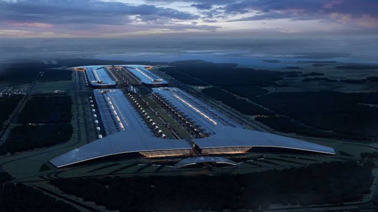
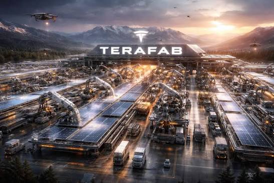
Tesla and SpaceX have released a dramatic new rendering and video of Terafab, their planned semiconductor megafactory. The visuals look straight out of science fiction — a vast, futuristic complex that Elon Musk has described as the largest and most valuable building on Earth by far.
The update, shared widely on August 6, 2026 (including by accounts like Sawyer Merritt), shows the scale and ambition of the project more clearly than ever.
What Is Terafab?
Terafab is a vertically integrated semiconductor fabrication plant being developed jointly by Tesla and SpaceX (with earlier involvement from xAI and a partnership with Intel). The name reflects its core goal: producing more than one terawatt (1 trillion watts) of AI compute capacity per year.
Unlike traditional fabs that specialize in one part of the process, Terafab aims to bring chip design, fabrication (including advanced lithography), memory production, advanced packaging, and testing under one roof. This vertical integration is intended to enable faster recursive improvements and secure supply for Musk’s companies.
The project was first publicly detailed by Elon Musk in March 2026. Current global chip production is described as far short of the demand expected from Optimus robots, Cybercabs, Full Self-Driving systems, and SpaceX’s planned space-based data centers.
Location and Unprecedented Scale
- Full-scale facility: Grimes County, Texas (near the Houston area / Gibbons Creek Reservoir site).
- Research/prototype fab: Already underway on the North Campus of Gigafactory Texas in Austin.
When complete, Terafab is planned to exceed 100 million square feet (roughly 3.6 square miles or about 10 million square meters). Comparisons shared online put it at roughly 50 times the size of the Pentagon and large enough to cover an area equivalent to a significant portion of a major city like Miami.
Musk has called it the most valuable building on the planet by a wide margin. The new renderings emphasize a highly automated, futuristic layout with references to Optimus robots, elevated roadways, Cybercabs, Tesla Semis, and other Tesla/SpaceX hardware integrated into the vision.

Investment and Jobs
Tesla and SpaceX have confirmed an initial investment of $16.8 billion for the first phase in Grimes County. Earlier SpaceX filings referenced higher potential figures (around $55 billion initial and up to $119 billion across phases), though the $16.8 billion figure is the first firm public commitment tied to the confirmed site.
The facility is expected to employ at least 3,000 people from Grimes and nearby Brazos County, with Texas state incentives and tax abatements involved. Tesla has already listed dozens of specialized job openings related to the project, covering process engineering (lithography, etch, deposition, CMP, implant, etc.), materials science, EHS, automation, and more.
What Chips Will Terafab Produce?
The plant is designed for two main categories of chips:
- Edge/inference chips optimized for terrestrial use in Tesla’s Optimus humanoid robots, Cybercab robotaxis, and vehicle Full Self-Driving systems.
- High-power chips designed for the harsh space environment to power SpaceX’s orbital/space-based data centers and AI satellites.
Intel is involved, with Musk previously noting the use of Intel’s 14A (1.4 nm) process technology for the full-scale facility. A smaller research fab at Giga Texas is intended to experiment and iterate before large-scale production.
Why Terafab Matters
Musk has repeatedly stated that existing and projected global semiconductor capacity will not meet the compute needs of Tesla’s robotics and autonomy plans combined with SpaceX’s space compute ambitions. Without dedicated capacity, those programs would be constrained.
By controlling more of the supply chain and co-locating design through packaging, the companies aim for faster iteration cycles. Success would also mark a major expansion of advanced semiconductor manufacturing in the United States.
The newly released rendering has generated significant attention for its scale and sci-fi aesthetic, reinforcing the long-term vision of abundant AI compute both on Earth and in space.
This is one of the most ambitious manufacturing projects currently planned. The new visuals make the scale feel more concrete — and more ambitious — than ever.